Maximum Power Point Tracker
Table of Contents
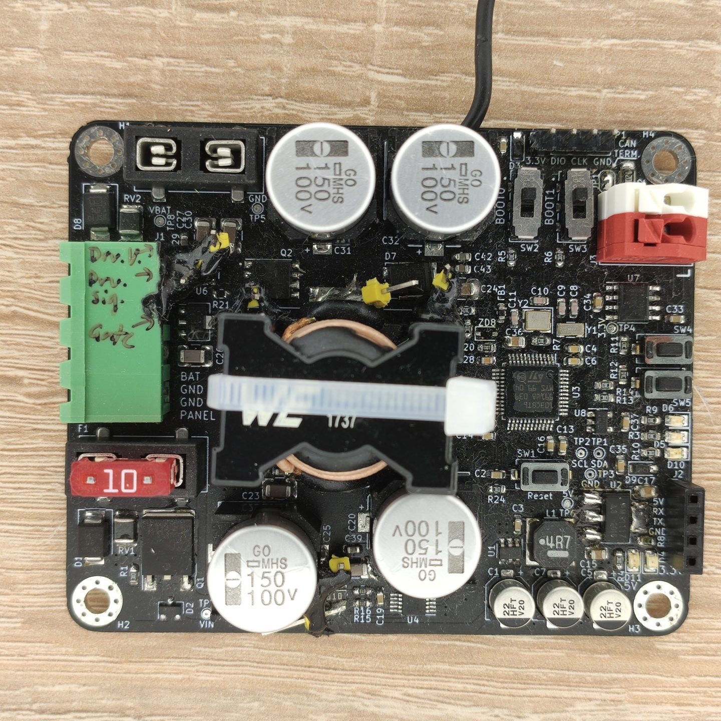
This is a MPPT I designed for my university's solar boat team.
See the project's GitHub repo here!
Overview
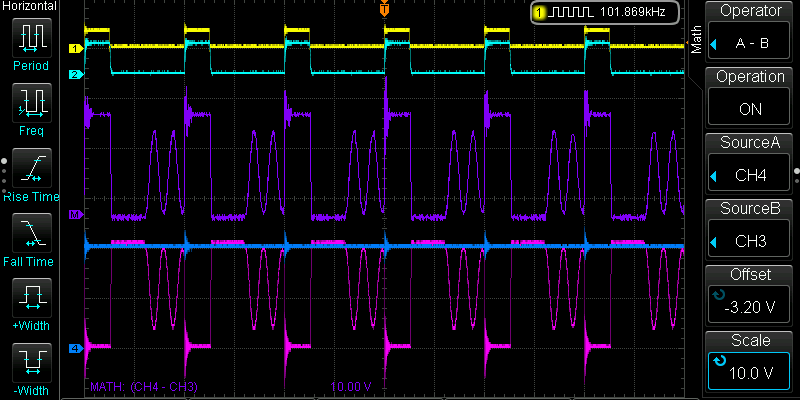
This design is capable of boosting voltages ranging from 16V to 36V up to >= 50V @ over 300W.
It's efficiency is about 95% or greater at relevant power-levels.
Hardware
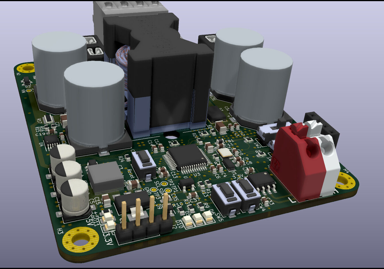
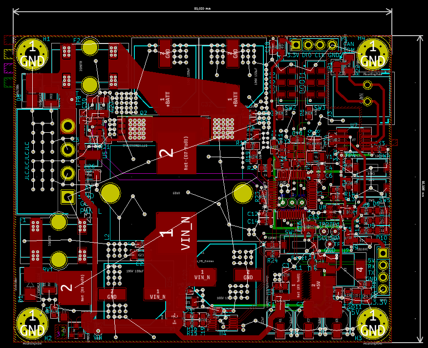
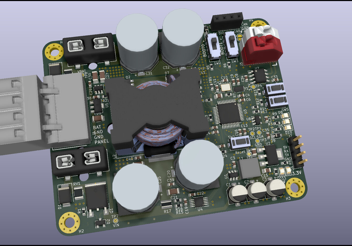
I designed the PCB in KiCAD. It's a four layer design due to the high power / current it has to handle. Another benefit is the improved EMC-performance.
The brains of the MPPT is an STM32F103 which runs a preturb and observe algorithm.
Input voltages within the range of 16V to 36V are boosted up to 50V (higher voltages are possible). The input power is monitored with an INA226.
All components have plenty of headroom but I have only pushed the design up to 150W for short periods of time due to my limited test-equipment.
Images
Here are some additional images of the project.
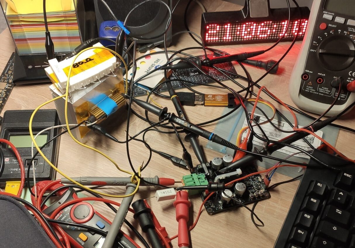
Testing of the latest revision
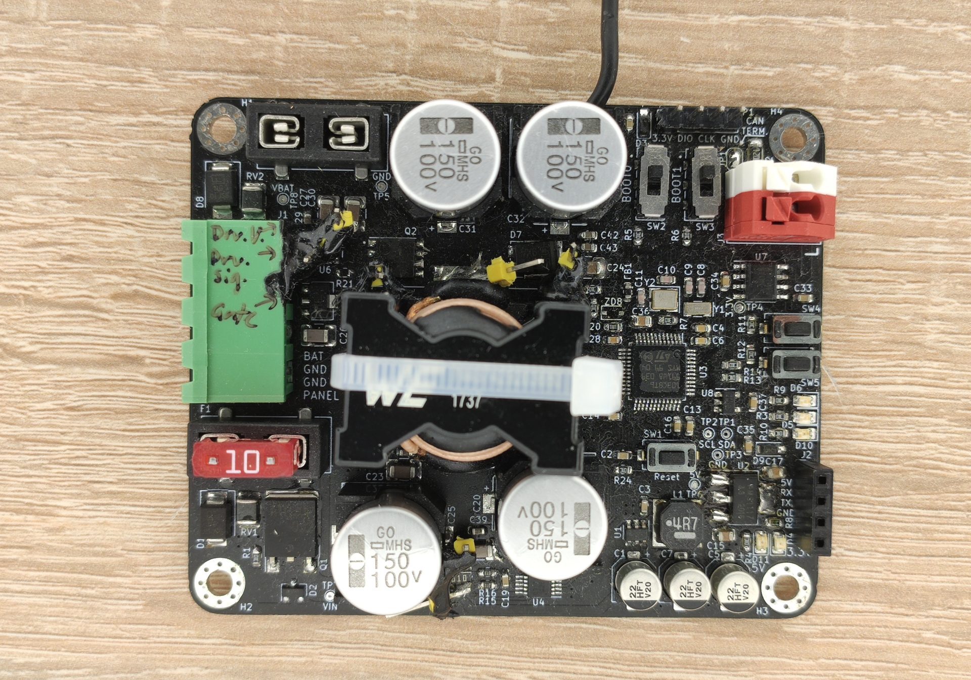
The current revision of the board with many test headers soldered on to make probing easier.
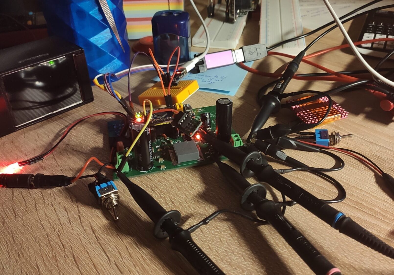
The last image shows the very first revision of the PCB design. Back when I designed it, I had significantly less experience.
Many lessons were learned and the whole PCB for the next revision was designed from the ground up. Many components were changed thanks to the information gathered from testing revision 1.
