
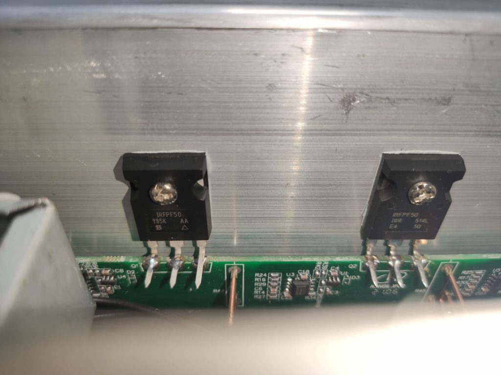
Note that the legs of the left MOSFET seem to be clean (no solder on them), where as the right MOSFET has a lot of solder on it’s legs. I presume that the right FET has been recycled from e-waste, just as the ones in the image above.
My thoughts:
Disclaimer: I haven’t tested the load at all.
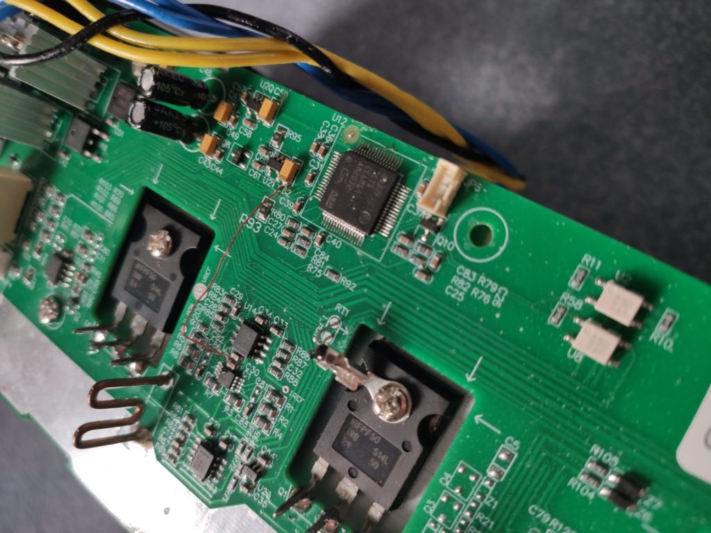
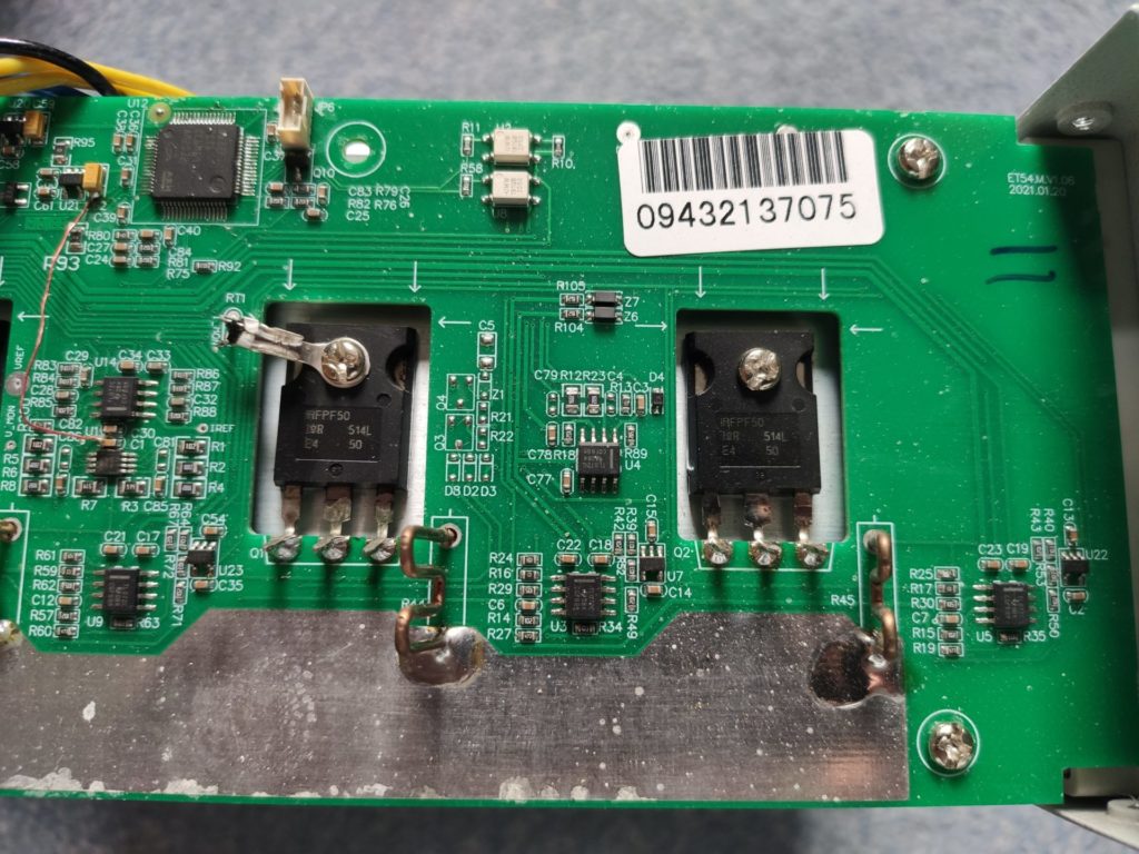
In total there are six MOSFETs. The packages differ between some of them. At least four of them appear to be recycled.
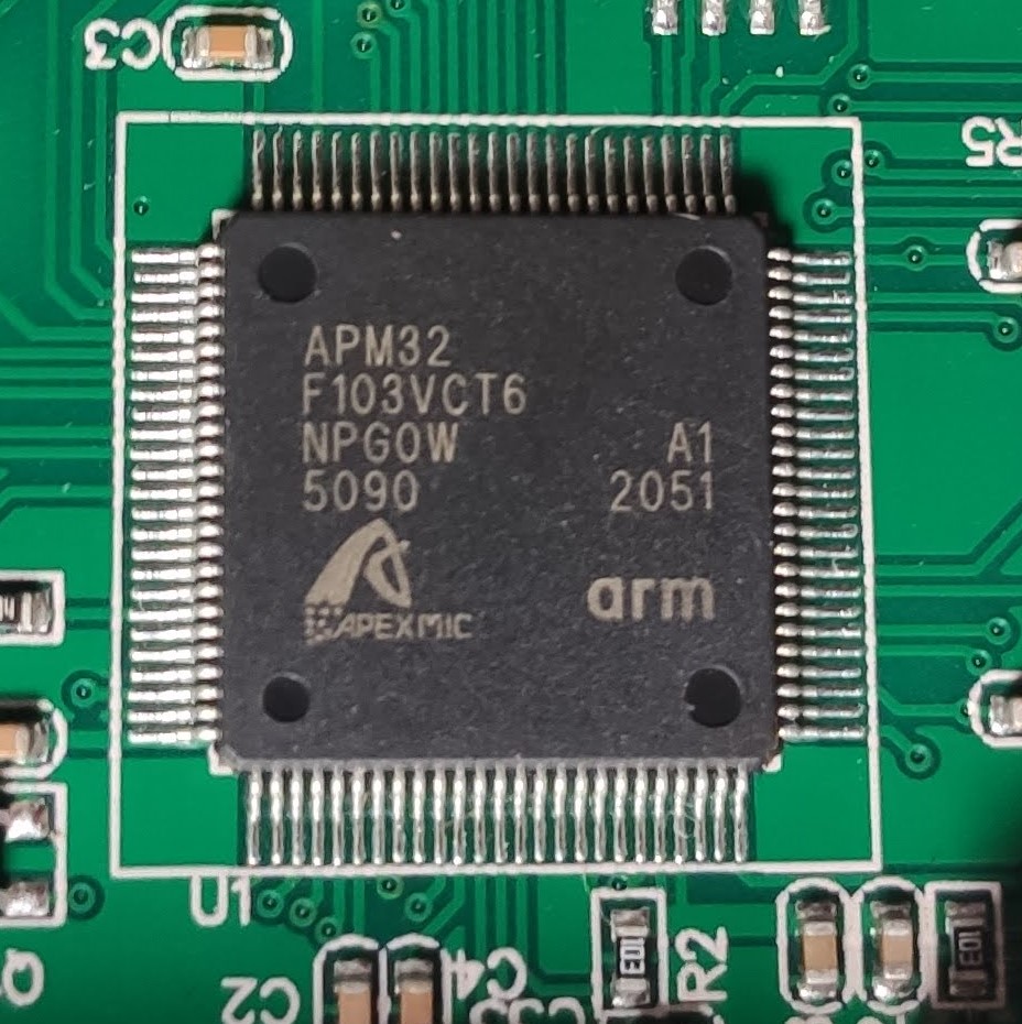
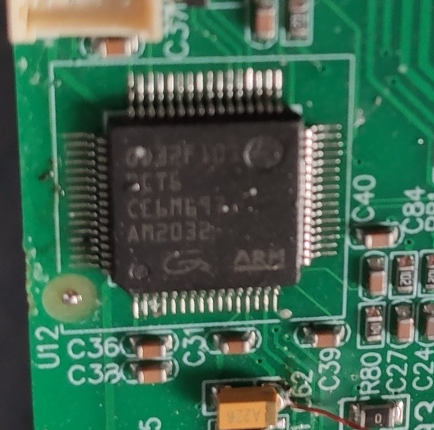
The Microcontrollers are clones of ST µControllers… Assuming the clones are good, there should not be any problems. The current Semiconductor shortage is very likely to blame for the decision to use cloned parts. Hopefully the manufacturer has done lots of testing (which is not very likely).
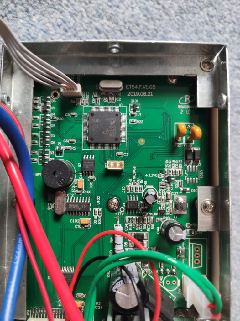
There is quite a lot of dust and overall dirt inside the unit.
Read more about the unit in this thread on the EEVBlog.
This short post doesn’t aim to be a review, but rather a collection of some thoughts and images I’d have liked to have before deciding on the purchase.
Thank you for the transparency! This kind of ‘internal audit’ is invaluable for the community, especially for those considering these budget power units. As an Electrical Engineering student at Telkom University Surabaya, I value your documentation of these red flags it definitely changes how I assess the value of such hardware